Download: 1.1.1 Structure and function of the processor
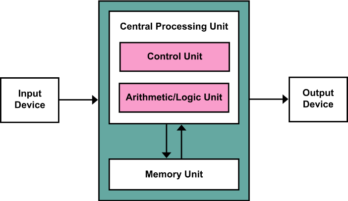
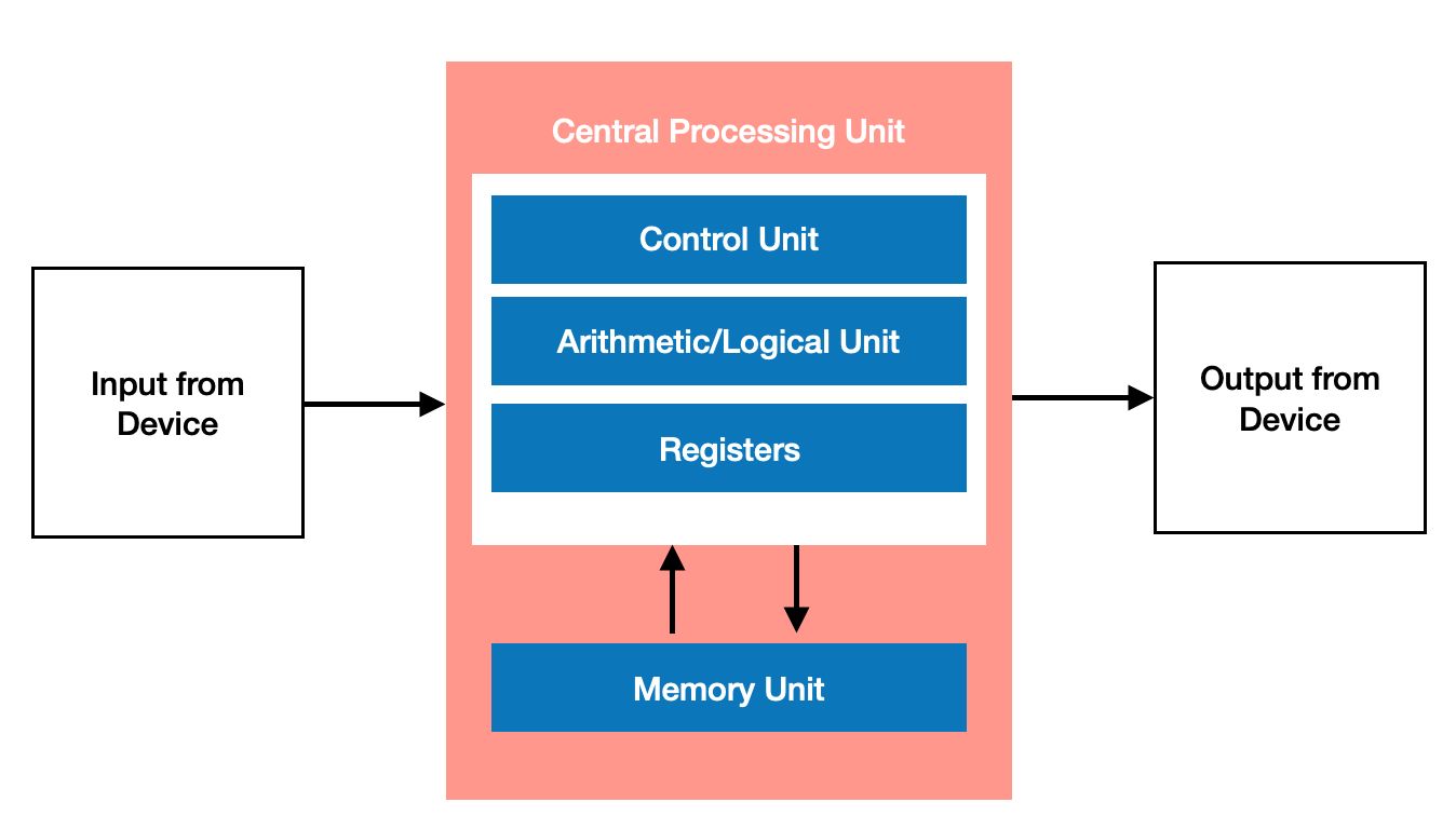
The Central Processing Unit (CPU)
The purpose of the CPU is to execute instructions in a computer system through the fetch-decode-execute cycle. It is where all the searching, sorting, calculating and decision making takes place in the computer.
The Arithmetic Logic Unit (ALU) – This performs all the arithmetic and logical operations of the CPU.
- Arithmetic part: Performs the calculations on data. For example: Addition, Subtraction, Multiplication and division on fixed or floating point numbers.
- Logic Part. Deals with logical operations. For example: Comparisons (Greater/Less than) & Boolean Operations such as AND, OR, NOT & XOR.
- It can also perform Shift Operations, which is shifting bits to the left or right within a register.
The Control Unit (CU) – Decodes and manages the execution of instructions using control signals to coordinate movement of data through the processor and other parts of the computer.
- Made up of two parts. The clock & the decoder, which coordinates the CPU’s activity. The decoder, which decodes the programs instructions.
- Manages & monitors hardware on the computer to ensure the correct data goes to the correct hardware.
- Manages the input & output signals ensuring these are dealt with correctly.
- Synchronises actions using an inbuilt clock.
- Manages the Fetch-Decode-Execute (FDE) Cycle
Registers: – These are special memory locations in the processor that temporarily store data and control information. They provide faster access to data compared to RAM in order to perform specific purposes during the FDE cycle when frequent access is required.
- Program Counter (PC): – Controls the sequence in which the instructions are retrieved and executed. It also stores the address of the next instruction to be processed. This address is then passed to the Memory Address Register (MAR) at the start of each instruction cycle. The PC is then incremented by one, which automatically moves on to the next instruction in the program.
- Accumulator (ACC): – Stores the output of the ALU. Located in the ALU, this is temporary storage of intermediate results of the ALU.
- General Purpose Register (GPR): – Used to temporarily store data being used rather than sending data to and from the comparatively much slower memory (RAM).
- Memory Address Register (MAR): – Holds the address of the memory location that is going to be accessed, which is copied from the Program Counter.
- Memory Data Register (MDR): – Stores the data that is to be written or has been retrieved from memory. Also known as the Memory Buffer Register.
- Current Instruction Register (CIR): – Stores the most recently fetched data to be decoded and executed into opcode & operand.
- Opcode is the first part of the instruction decoded that specifies what operation the Control Unit needs to perform.
- Opand is the remainder of the computer instruction, which specifies what data is to be manipulated or operated on, while at the same time representing the data itself.
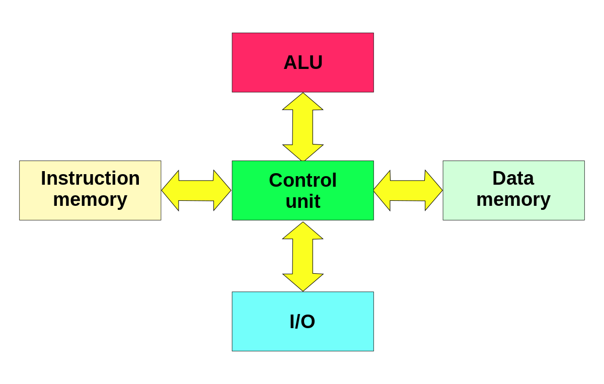
Buses:
A bus is a parallel group of communication channel wires, which are able to transmit data in groups of bits together from one register to another in the processor. Typically consists of 8, 16, 32, or 64 lines.
The Data Bus:
- This provides a bi-directional path for data/instructions being transmitted from one register to another between the areas of the processor and memory.
- Typically consisting of 8, 16, 32 or 64 separate lines.
The Address Bus: –
- This carries the memory location address of the register where the data is being transmitted to or from.
- Memory is divided up internally into units called words. A word is a fixed size group of digits, typically 16, 32 or 64 bits. This is handled as a unit by the processor.
- Each word in a memory has its own specific address. The Address Bus transmits the memory addresses of ‘words’ that are used as Opand in program instructions. This is so the data can be retrieved and send back to the processor.
- When an instruction has been executed and the result has been stored in a certain memory location. It is then transmitted along the Data Bus.
The Control Bus:
- This transmit control signals from the Control Unit to allow synchronisation of signals to the rest of the processor.
- The purpose of the control bus is to transmit command, timing and specific status information between system components.
- It is a bi-directional bus, meaning that singals can be carried in both directions.
- It consists of a bunch of control lines:
- Bus Request: Shows that a device is requesting the use of the Data Bus.
- Bus Grant: Shows that the CPU has granted access to the Data Bus.
- Memory Write: Causes data on the Data Bus to be written into the addressed location.
- Memory Read: Causes data from the addressed location to be placed on the Data Bus.
- Interrupt Request: Shows that a device is requesting access to the CPU.
- Clock: Used to synchronise operations.
Fetch-Decode-Execute Cycle: (FDE)
Fetch Stage: (Fetches Instructions)
- The memory location is copied from the Program Counter (PC) to the Memory Address Register (MDR) along the Address Bus.
- The instruction stored in the Memory Address Register is copied to the Memory Data Register (MDR) along the Data Bus.
- The Program Counter is incremented by one, which then the fetch signal is sent along the control bus. This points towards to the address of the next instruction in order to prepare for the next cycle.
- The contents of the Memory Data Register and the Accumulator (ACC) are then sent to the Arithmetic Logic Unit (ALU) and the results are then stored back into the Accumulator.
Decode Stage: (Decodes Instruction)
- Loads instruction from the address located in the Memory Address Register, which is pointed to the Memory Data Register.
- The instruction is copied from the Memory Data Register to the Current Instruction Register (CIR).
- The instruction is then decoded into opcode and operand by the Control Unit (CU) in the Current Instruction Register.
Execute Stage: (The instruction is completed)
- The appropriate instruction in opcode is carried out onto the data in operand by the processor.
Factors that affect the performance of the CPU:
Word Length: – The Word is the number of bits in a single memory location.
- The Word length is the same as the width of the bus.
- A larger word length means more data can be processed in a single operation.
- E.g 32 bit or 64 bit processors.
Clock Speed: – The number of instructions a single processor core can carry out per second measured in Hertz.
- The average desktop computer’s processor will be somewhere around 3.5Ghz, which is 3.5 billion instructions per second. 1 Hz is equal to one instruction per second.
- The higher the clock speed, the greater the number of instructions can be carried out per second.
- This is pushing/increasing the clock speed over the manufacture’s intended/original speed. It can make a CPU run at a higher speed than the factory set rate, but it can be risky. It can cause a CPU to overheat, crash or cause permanent damage. Normally a higher performance cooling system are required to withstand against the heat of the processor.
Number of Cores: – Each core in a processor can process data independently.
- The more cores a CPU has, the more instructions that can be carried out at once. This makes it faster to process a batch of data.
- When multitasking, different cores can run different applications. Multiple cores can also work on the same problem.
Cache Size: – Cache is data storage inside the CPU that is much faster compared to Random Access Memory (RAM)
- A large CPU cache gives the CPU faster access to more data it needs to process.
- Cache stores data/instructions that is more likely to be accessed regularly, this increases the speed of the processors as it prevents the need to access Random Access Memory, which is slower.
- Cache Levels.
- Level One Cache: Extremely fast but small. (Between 2 to 64KB of space)
- Level Two Cache: Fast and medium sized. (256KB to 2MB of space)
- Level Three Cache: Still fast, but slower compared to other levels. Also has the largest storage space.
Pipelining: (The implementation technique where multiple instructions are overlapped in execution)
- Allows one instructions to be fetched as the previous one is being decoded and the one before that is being executed.
- It does not decrease the time taken for individual instruction execution. Instead, it increases instruction throughput. Throughput is determined by how often an instruction exits the pipeline.
- The throughput of pipelining is difficult to predict as it depends on the type of processor being used. The longer the pipeline, worse the problem of hazard for branch instructions.
Processor Architecture: (An architecture is a design for the basic structure of a computer system)
Von Neumann: (Specifics the basic components of the computer and processor)
- Data & instructions are stored in the same memory.
- Same bus is used for data & instructions
- To get an instruction and the data. It takes two ‘fetch’ operations.
Harvard:
- Data & instructions are stored in different memory areas.
- Data & instructions travel along different buses.
- The CPU can fetch data & instructions at the same time
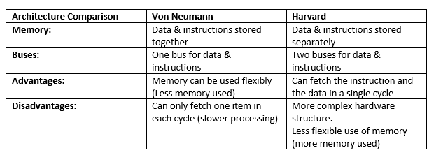
Modified Harvard/Contemporary Processor Architecture: (elements used from both architectures)
- Data & instructions share the same memory space.
- Data & instructions travel down different buses.
- Gives the best of both architectures
![]()